
A practical look at how continuity across design, sourcing, manufacturing, testing and system integration improves production readiness.
OEMs are under pressure to shorten development cycles while managing greater product complexity, tighter form factors and unpredictable component availability. Yet many electronics programs still move through separate design, sourcing, PCB assembly, testing and system-integration environments. Every handoff creates another opportunity for assumptions to change and feedback to arrive late.
A prototype may pass functional testing and still be difficult to manufacture repeatedly. A component approved during development may not remain available for production. A PCBA may work on the bench but encounter thermal, mechanical or cabling constraints inside its enclosure. These are continuity problems across the product-realization process.
End-to-end Electronics System Design and Manufacturing (ESDM) reduces production risk by connecting how a product is designed with how it will be sourced, assembled, tested, integrated and controlled through production.
Electronics programs rarely lose time because one discipline is absent. They lose time when decisions made in one stage are transferred without enough manufacturing, supply-chain or system-level context.
The commercial impact depends on when the issue is discovered. After design release or during NPI, correction may require another build, another validation cycle and coordination across several suppliers.
A PCB layout must achieve the intended electrical performance, but it must also support repeatable assembly, inspection and test. This is why design for manufacturability in PCB assembly should begin before the design is frozen—not after a production issue appears.
DFM examines whether the design can be built consistently. Design for Testability (DFT) examines whether that build can be verified efficiently. Together, they connect engineering intent to the realities of the production process.
The objective is not to simplify every design. It is to make unavoidable complexity visible early enough for engineering and manufacturing teams to manage it deliberately.
Component sourcing is often treated as a procurement activity that begins after engineering is complete. In practice, sourcing decisions affect redesign risk, production continuity, and configuration control.
Parts selected for a prototype may carry long lead times, limited availability, high minimum-order quantities, or approaching end-of-life status. A rushed substitution may fix availability while creating a new electrical, thermal, mechanical or compliance question.
An integrated ESDM workflow brings supply chain input into engineering earlier. BOM reviews identify availability and lifecycle exposure, while alternatives can be assessed before shortages force an urgent decision. If a change is required, engineering, purchasing, quality, and manufacturing can evaluate the same revision and its effect on the finished product.
During turnkey PCB assembly, the question shifts from whether one board can work to whether an approved process can produce the same result across every build.
Repeatability depends on more than placement accuracy. Material control, solder-paste deposition, component handling, reflow profiling, through-hole processing and documented workmanship criteria all contribute to process stability.
Inspection should match the design risk. Solder Paste Inspection (SPI) verifies deposition before placement. Automated Optical Inspection (AOI) identifies visible anomalies, while X-ray can evaluate hidden interconnects. In-circuit and functional testing provide different forms of electrical verification.
No single method creates quality by itself. Quality comes from controlled processes, appropriate inspection coverage, traceability, and a defined response to variation.
When testing is introduced late, teams may find critical nodes inaccessible, programming interfaces obstructed, or system behavior difficult to separate from a board-level fault. Diagnosis and validation then take longer.
An early test strategy defines what must be verified at each stage, which fixtures or software are required, and how results will be recorded. It also connects board-level testing with final system acceptance.
This makes failures easier to isolate before a board enters an enclosure, while cable, power, firmware and thermal interactions can be evaluated at system level. Test data becomes part of production control—not merely a final pass-or-fail gate.
During box build, the PCBA begins interacting with cable harnesses, connectors, enclosures, displays, power assemblies, thermal interfaces and mechanical hardware. Firmware, labeling, and final configuration may also enter the build record.
This stage exposes dependencies that board-level validation cannot reproduce fully. Cable routing can affect airflow; connector orientation can create assembly strain, enclosure tolerances can influence fit, and grounding or power-distribution decisions can affect system behavior. Separate subassemblies must now work as one controlled system.
For this reason, electromechanical box-build services should not be treated as packaging after PCBA. Box build is the stage where product-level manufacturability and system-level readiness are proven together.
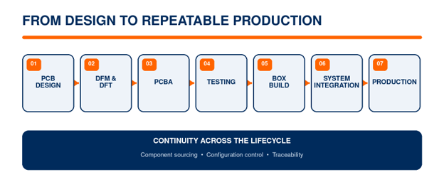
The workflow is not rigidly one-way. Findings from sourcing, assembly, test and system integration must return to the relevant engineering decision. The advantage is faster, controlled iteration using shared product data.
Using one partner for several activities creates value only when those activities operate as one product-realization process. Design, sourcing, manufacturing, quality and integration teams must work from controlled information and act on one another’s feedback.
For OEMs, these outcomes influence engineering workload, launch confidence, change-control risk, supplier-management effort and the ability to scale without rebuilding knowledge between vendors.
The answers reveal whether a provider offers a service list or an integrated operating model.
At Aimtron, product design services, PCB assembly, testing, electromechanical box build and system integration are connected within one product-realization journey. Manufacturing, quality and integration requirements can therefore inform engineering earlier as products move from prototype and NPI into repeatable production.
The objective is straightforward: make the product not only functional, but manufacturable, testable, traceable and ready to perform as a complete system.
Planning a new electronic product or preparing for production? Explore how Aimtron can support your journey from PCB design to system integration.